Tuesday, 11 July 2023

Laser pulse creates exotic order in quantum material


Water flows, ice is rigid—this clear difference between the liquid and solid state of substances is part of our everyday experience. It follows from the very regular arrangement of atoms and molecules in crystalline solids, which is lost when they melt. Less clear, however, is the structure of "liquid crystals"—highly interesting states that combine order and disorder in such a way that important applications such as LCDs (liquid crystal displays) are possible.

Researchers from the Max Planck Institute (MPI) for Multidisciplinary Sciences in Göttingen, in collaboration with colleagues from Kiel University (CAU), Deutsches Elektronen Sychrotron DESY and University of Göttingen have now successfully created a state in a crystalline material that—similar to the structure of liquid crystals—can be described as neither clearly liquid nor clearly crystalline.

The studied layered crystal, grown in Kiel by Kai Rossnagel's team, professor at CAU and leading scientist at DESY, is characterized by a minimal distortion of the crystal structure at room temperature. This is due to the special structure of the crystal, in which thin layers of metal and sulfur atoms are stacked on top of each other and only weakly bound.

If these layers are now bombarded with ultrashort laser flashes, the distortion changes its orientation within a trillionth of a second, abruptly increasing the electrical conductivity of the material. Although both types of distortions have an ordered structure and associated crystalline properties, a highly disordered state can be observed during the transition.
Short snapshot: State disappeared after nanosecond fraction

"After exciting the material with light, the atoms in the crystal structure have yet to find their new, slightly different positions. This transforms the material into an unusually disordered, so-called hexatic state," says Till Domröse, Ph.D. student at MPI and first author of the study now published in the journal Nature Materials.

"This state is otherwise mainly observed in liquid crystals. In our experiments, however, it is extremely volatile and has already disappeared after the fractions of a nanosecond." Making the hexatic state visible placed high demands on the measurement technology used. On the one hand, for example, a very fast temporal resolution is required to take a sufficiently short snapshot. On the other hand, the structural changes in the material are so subtle that they can only be seen with a very high sensitivity to atomic positions. Electron microscopes in principle provide the necessary spatial resolution, but are typically not fast enough.

In recent years, the Göttingen team led by Max Planck Director Claus Ropers has closed this gap by developing an "ultrafast" electron microscope capable of imaging even unimaginably rapid processes in the nanocosmos. "This microscope was also used in these experiments and enabled us to capture the unusually ordered phase and its temporal evolution in a series of images," Ropers explains. "At the same time, we developed a new high-resolution diffraction mode that will be essential for studying many other functional nanostructures."


Unique layered crystals

"The highly complex dynamics that take place in this type of layered crystal offer numerous scientific questions and possible applications," says Rossnagel, member of the speaker group of the priority research area KiNSIS (Kiel Nano, Surface and Interface Science) at CAU and lead scientist at the German Electron Synchrotron DESY in Hamburg. "The basis are fascinating network-like structures, which we can only develop and study in close collaboration with state-of-the-art research infrastructures such as at the MPI in Göttingen and DESY in Hamburg. This enables excellent research on quantum materials in northern Germany."

"The highly complex dynamics that take place in this type of layered crystal offer numerous scientific questions and possible applications," says Rossnagel, a member of the speaker group of the research focus KiNSIS (Kiel Nano, Surface and Interface Science) at CAU. "The basis is fascinating network-like structures that we can only develop and investigate in close cooperation with state-of-the-art research infrastructures such as at the MPI in Göttingen and DESY in Hamburg. This enables excellent research on quantum materials in northern Germany."

These special crystals have been grown in Kiel since the early 1980s. Close ties between CAU and DESY have existed for just as long, and are now institutionalized in the Ruprecht-Haensel Laboratory. "DESY's high-precision nanoanalytics with the PETRA III and FLASH facilities have contributed decisively to the high quality of our crystals and helped ensure that we receive enquiries from all over the world," Rossnagel continues. Studies like this one with the MPI in Göttingen, in which a novel state was discovered in a quantum material, also open up perspectives for future collaboration with DESY research groups to better understand new quantum materials.

#QuantumMaterial #ExoticOrder #LaserPulse #QuantumPhysics

Visit:https://quantumtech.sfconferences.com/

Award Nomination: https://x-i.me/quawards
Award Registration: https://x-i.me/quareg2

Twitter:https://twitter.com/quantumtech23
Instagram:https://www.instagram.com/sahara_navi/


Friday, 7 July 2023

Scientists propose an all-optical labeling method for encrypted fiber optic tags


Fiber sensing scientists from Shenzhen University have developed an encrypted fiber optic tag that can be used for all-optical labeling and recognition of optical transmission channels such as access networks.

Publishing in the journal International Journal of Extreme Manufacturing, the team led by researchers based at the Guangdong and Hong Kong Joint Research Center for Optical Fiber Sensors proposed an all-optical labeling method with encryption property, which uses the feature information and spatial distribution of fiber Bragg grating arrays to flexibly store different coding sequences.

Unlike traditional optical link labeling methods, the all-fiber tag proposed by the team fully utilizes the characteristics of the optical link to achieve all-optical reading, recognition, and restoration of link information. The findings could have a significant impact on the maintenance of optical distribution networks.

The fiber optic tag is based on a fiber Bragg grating array prepared by femtosecond laser direct writing. By cleverly utilizing the spatial distribution, reflectivity, and reflection wavelength of the gratings, the tag can carry rich information. When using an optical time-domain reflectometer for reading, a specific administrator can perform complete and error-free information recovery.

One of the lead researchers, Professor Changrui Liao, commented, "This study developed a method for all-optical link encryption labeling and recognition. Faced with the increasing number of optical transmission links, traditional physical labels have high labor costs and are prone to waste port resources, making it difficult to meet efficient and stable link labeling requirements. All of these indicate that this fiber optic tag will have broad market application prospects."

One-off printed physical labels or handwritten symbols can be used to number and distinguish links, however, these highly manual methods face significant challenges in the information age.

First author Mr. Zhihao Cai explained, "Our work provides a reliable and efficient encryption labeling method for optical signal transmission link labeling. The use of femtosecond laser direct writing can achieve rapid mass production of tags, which are very helpful for obtaining dumb information for optical network users."

The team prepared a fiber Bragg grating array using femtosecond laser multi-pulse exposure, which can control the characteristics of different grating fragments, such as reflectivity. By utilizing the reflected signal of the grating to increase the number of switch states that the fiber optic tag can represent, the storage capacity of the fiber tag is improved.

Due to the distribution and reflection characteristics of the grating, there are many possibilities for fiber optic tags to read and recover information. Therefore, only specific management personnel can obtain correct optical link information to prove that fiber optic tags have sufficient security.

Professor Yiping Wang said, "This work fully demonstrates the flexibility of the femtosecond laser direct writing technology, by adjusting the number of femtosecond laser pulse exposures to achieve regulation of the reflection characteristics of each encoded grating fragment, ultimately giving the proposed fiber tag greater capacity and application potential. It is a fascinating and practical task for maintaining existing optical networks."

#OpticalLabeling #FiberOpticTags #EncryptionTechnology #SecureCommunication #OpticalCommunication #DataSecurity #ScientificResearch #Innovation #Photonics #OpticalTechnology


Thursday, 6 July 2023

Quantum neural networks: An easier way to learn quantum processes


EPFL scientists show that even a few simple examples are enough for a quantum machine-learning model, the "quantum neural networks," to learn and predict the behavior of quantum systems, bringing us closer to a new era of quantum computing.

Imagine a world where computers can unravel the mysteries of quantum mechanics, enabling us to study the behavior of complex materials or simulate the intricate dynamics of molecules with unprecedented accuracy.

Thanks to a pioneering study led by Professor Zoe Holmes and her team at EPFL, we are now closer to that becoming a reality. Working with researchers at Caltech, the Free University of Berlin, and the Los Alamos National Laboratory, they have found a new way to teach a quantum computer how to understand and predict the behavior of quantum systems. The research has been published in Nature Communications.
Quantum neural networks (QNNs)

The researchers worked on "quantum neural networks" (QNNs), a type of machine-learning model designed to learn and process information using principles inspired by quantum mechanics in order to mimic the behavior of quantum systems.

Just like the neural networks used in artificial intelligence, QNNs are made of interconnected nodes, or "neurons," that perform calculations. The difference is that, in QNNs, the neurons operate on the principles of quantum mechanics, allowing them to handle and manipulate quantum information.

"Normally, when we teach a computer something, we need a lot of examples," says Holmes. "But in this study, we show that with just a few simple examples called 'product states' the computer can learn how a quantum system behaves even when dealing with entangled states, which are more complicated and challenging to understand."
Product states

The "product states" that the scientists used refer to a concept in quantum mechanics that describes the specific type of state for a quantum system. For example, if a quantum system is composed of two electrons, then its product state is formed when each individual electron's state is considered independently, and then combined.

Product states are often used as a starting point in quantum computations and measurements because they provide a simpler and more manageable framework for studying and understanding the behavior of quantum systems, before moving on to more complex and entangled states, where the particles are correlated and cannot be described independently.
Better quantum computers ahead

The researchers demonstrated that by training QNNs using only a few of these simple examples, computers can effectively grasp the complex dynamics of entangled quantum systems.

Holmes explains, "This means that [we] might be able to learn about and understand quantum systems using smaller, simpler computers, like the near-term intermediary scale [NISQ] computers we're likely to have in the coming years, instead of needing large and complex ones, which may be decades away."

The work also opens up new possibilities for using quantum computers to solve important problems like studying complex new materials or simulating the behavior of molecules.

Finally, the method improves the performance of quantum computers by enabling the creation of shorter and more error-resistant programs. By learning how quantum systems behave, we can streamline the programming of quantum computers, leading to improved efficiency and reliability. "We can make quantum computers even better by making their programs shorter and less prone to errors," says Holmes.

#QuantumNeuralNetworks #QuantumProcesses #QuantumComputing #MachineLearning #ArtificialIntelligence

Wednesday, 5 July 2023

Scientists discover Rydberg moiré excitons


The Rydberg state is widespread in a variety of physical platforms such as atoms, molecules, and solids. In particular, Rydberg excitons are highly excited Coulomb-bound states of electron-hole pairs, first discovered in the semiconductor material Cu2O in the 1950s.

In a study published in Science, Dr. Xu Yang and his colleagues from the Institute of Physics of the Chinese Academy of Sciences (CAS), in collaboration with researchers led by Dr. Yuan Shengjun of Wuhan University, have reported observing Rydberg moiré excitons, which are moiré-trapped Rydberg excitons in the monolayer semiconductor WSe2 adjacent to small-angle twisted bilayer graphene (TBG).

The solid-state nature of Rydberg excitons, combined with their large dipole moments, strong mutual interactions and greatly enhanced interactions with the surroundings, holds promise for a wide range of applications in sensing, quantum optics, and quantum simulation.

However, researchers have not fully exploited the potential of Rydberg excitons. One of the main obstacles lies in the difficulty of efficiently trapping and manipulating Rydberg excitons. The rise of two-dimensional (2D) moiré superlattices with highly tunable periodic potentials provides a possible way forward.

In recent years, Dr. Xu Yang and his collaborators have worked on exploring the application of Rydberg excitons in 2D semiconducting transition metal dichalcogenides (such as WSe2). They have developed a new Rydberg sensing technique that exploits the sensitivity of Rydberg excitons to the dielectric environment to detect the exotic phases in a nearby 2D electronic system.
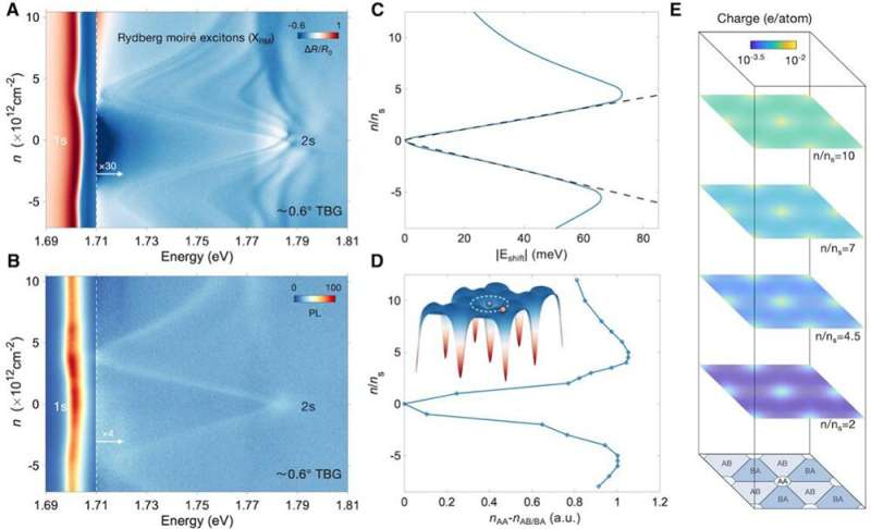
Spectroscopic evidence of the Rydberg moiré exciton formation in WSe2 adjacent to 0.6° TBG and numerical calculations of the spatial charge distribution in TBG at different doping levels. Credit: IOP

In this study, using low-temperature optical spectroscopy measurements, the researchers first found the Rydberg moiré excitons manifesting as multiple energy splittings, a pronounced red shift, and a narrowed linewidth in the reflectance spectra.

Using numerical calculations performed by the group from Wuhan University, the researchers attributed these observations to the spatially varying charge distribution in TBG, which creates a periodic potential landscape (so-called moiré potential) for interacting with Rydberg excitons.

The strong confinement of Rydberg excitons is achieved by the largely unequal interlayer interactions of the constituent electron and hole of a Rydberg exciton due to the spatially accumulated charges centered in the AA-stacked regions of TBG. The Rydberg moiré excitons thus realize electron–hole separation and exhibit the character of long-lived charge-transfer excitons.

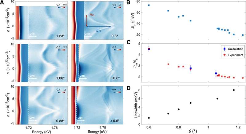
Twist angle dependences and crossover to the strong-coupling regime. Credit: IOThe researcher demonstrated a novel method of manipulating Rydberg excitons, which is difficult to achieve in bulk semiconductors. The long-wavelength (tens of nm) moiré superlattice in this study serves as an analog to the optical lattices created by a standing-wave laser beam or arrays of optical tweezers that are used for Rydberg atom trapping.

In addition, tunable moiré wavelengths, in-situ electrostatic gating, and a longer lifetime all ensure great controllability of the system, with a strong light–matter interaction for convenient optical excitation and readout.

This study may provide new opportunities for realizing the next step in Rydberg–Rydberg interactions and coherent control of Rydberg states, with potential applications in quantum information processing and quantum computation.


Tuesday, 4 July 2023

Novel 'toggle-switch' could lead to more versatile quantum processors with clearer outputs


What good is a powerful computer if you can't read its output? Or readily reprogram it to do different jobs? People who design quantum computers face these challenges, and a new device may make them easier to solve.

The device, introduced by a team of scientists at the National Institute of Standards and Technology (NIST), includes two superconducting quantum bits, or qubits, which are a quantum computer's analog to the logic bits in a classical computer's processing chip. The heart of this new strategy relies on a "toggle switch" device that connects the qubits to a circuit called a "readout resonator" that can read the output of the qubits' calculations.

This toggle switch can be flipped into different states to adjust the strength of the connections between the qubits and the readout resonator. When toggled off, all three elements are isolated from each other. When the switch is toggled on to connect the two qubits, they can interact and perform calculations. Once the calculations are complete, the toggle switch can connect either of the qubits and the readout resonator to retrieve the results.

Having a programmable toggle switch goes a long way toward reducing noise, a common problem in quantum computer circuits that makes it difficult for qubits to make calculations and show their results clearly.

"The goal is to keep the qubits happy so that they can calculate without distractions, while still being able to read them out when we want to," said Ray Simmonds, a NIST physicist and one of the paper's authors. "This device architecture helps protect the qubits and promises to improve our ability to make the high-fidelity measurements required to build quantum information processors out of qubits."

The team, which also includes scientists from the University of Massachusetts Lowell, the University of Colorado Boulder and Raytheon BBN Technologies, describes its results in a paper published June 26 in Nature Physics.

Quantum computers, which are still at a nascent stage of development, would harness the bizarre properties of quantum mechanics to do jobs that even our most powerful classical computers find intractable, such as aiding in the development of new drugs by performing sophisticated simulations of chemical interactions.

However, quantum computer designers still confront many problems. One of these is that quantum circuits are kicked around by external or even internal noise, which arises from defects in the materials used to make the computers. This noise is essentially random behavior that can create errors in qubit calculations.

Present-day qubits are inherently noisy by themselves, but that's not the only problem. Many quantum computer designs have what is called a static architecture, where each qubit in the processor is physically connected to its neighbors and to its readout resonator. The fabricated wiring that connects qubits together and to their readout can expose them to even more noise.

Such static architectures have another disadvantage: They cannot be reprogrammed easily. A static architecture's qubits could do a few related jobs, but for the computer to perform a wider range of tasks, it would need to swap in a different processor design with a different qubit organization or layout. (Imagine changing the chip in your laptop every time you needed to use a different piece of software, and then consider that the chip needs to be kept a smidgen above absolute zero, and you get why this might prove inconvenient.)

The team's programmable toggle switch sidesteps both of these problems. First, it prevents circuit noise from creeping into the system through the readout resonator and prevents the qubits from having a conversation with each other when they are supposed to be quiet.

"This cuts down on a key source of noise in a quantum computer," Simmonds said.

Second, the opening and closing of the switches between elements are controlled with a train of microwave pulses sent from a distance, rather than through a static architecture's physical connections. Integrating more of these toggle switches could be the basis of a more easily programmable quantum computer. The microwave pulses can also set the order and sequence of logic operations, meaning a chip built with many of the team's toggle switches could be instructed to perform any number of tasks.

"This makes the chip programmable," Simmonds said. "Rather than having a completely fixed architecture on the chip, you can make changes via software."

One last benefit is that the toggle switch can also turn on the measurement of both qubits at the same time. This ability to ask both qubits to reveal themselves as a couple is important for tracking down quantum computational errors.

The qubits in this demonstration, as well as the toggle switch and the readout circuit, were all made of superconducting components that conduct electricity without resistance and must be operated at very cold temperatures. The toggle switch itself is made from a superconducting quantum interference device, or "SQUID," which is very sensitive to magnetic fields passing through its loop. Driving a microwave current through a nearby antenna loop can induce interactions between the qubits and the readout resonator when needed.

At this point, the team has only worked with two qubits and a single readout resonator, but Simmonds said they are preparing a design with three qubits and a readout resonator, and they have plans to add more qubits and resonators as well. Further research could offer insights into how to string many of these devices together, potentially offering a way to construct a powerful quantum computer with enough qubits to solve the kinds of problems that, for now, are insurmountable.

#QuantumComputing #QuantumProcessors #ToggleSwitch #Versatility #ClearOutputs

Monday, 3 July 2023

Scientists edge toward scalable quantum simulations on a photonic chip


Scientists have made an important step toward developing computers advanced enough to simulate complex natural phenomena at the quantum level. While these types of simulations are too cumbersome or outright impossible for classical computers to handle, photonics-based quantum computing systems could provide a solution.

A team of researchers from the University of Rochester's Hajim School of Engineering & Applied Sciences developed a new chip-scale optical quantum simulation system that could help make such a system feasible. The team, led by Qiang Lin, a professor of electrical and computer engineering and optics, published their findings in Nature Photonics.

Lin's team ran the simulations in a synthetic space that mimics the physical world by controlling the frequency, or color, of quantum entangled photons as time elapses. This approach differs from the traditional photonics-based computing methods in which the paths of photons are controlled, and also drastically reduces the physical footprint and resource requirements.

"For the first time, we have been able to produce a quantum-correlated synthetic crystal," says Lin. "Our approach significantly extends the dimensions of the synthetic space, enabling us to perform simulations of several quantum-scale phenomena such as random walks of quantum entangled photons."

The researchers say that this system can serve as a basis for more intricate simulations in the future.

"Though the systems being simulated are well understood, this proof-of-principle experiment demonstrates the power of this new approach for scaling up to more complex simulations and computation tasks, something we are very excited to investigate in the future," says Usman Javid '23 Ph.D., the lead author on the study.

Other co-authors from Lin's group include Raymond Lopez-Rios, Jingwei Ling, Austin Graf, and Jeremy Staffa.

#QuantumSimulations #PhotonicChip #ScalableComputing #QuantumComputing #QuantumTechnology #Photonics #QuantumInformation #QuantumPhysics #QuantumAdvancements #QuantumScience


Saturday, 1 July 2023

Researchers develop cryogenic integrated quantum entangled light source


The research team led by academician Guo Guangcan and Prof. Ren Xifeng from the University of Science and Technology of China (USTC) of the Chinese Academy of Sciences (CAS) achieved quantum photonic sources at cryogenic temperatures based on the spontaneous four-wave mixing (SFWM) effect. The results are published in Optica.

Quantum photonic integrated circuits (QPICs), with their extremely high phase stability and reconfigurability, are powerful platforms that have fueled a wide range of quantum information applications with significant building blocks and are becoming possible candidates to interface different quantum systems with hybrid integrated techniques.

Current investigations on QPICs mainly focus on operation at ambient temperatures, while many quantum components have to operate under cryogenic conditions. Additionally, quantum technologies must be mutually compatible for the sake of scalable photonic quantum computing and interfacing among different quantum systems. Therefore, QPICs that are designed at room temperature, especially those involving nonlinear processes, should be able to work in cryogenic environments.

The researchers set their eyes on the SFWM effect for its outstanding performance in a variety of nonlinear processes and quantum applications. They managed to make breakthroughs through studying the SFWM effect in an integrated silicon waveguide under cryogenic operation conditions. They revealed that the effect was still in good performance for generating quantum photonic sources.

Then, the researchers investigated the noises from the photon-pair source preparation with cryogenic photon-pairs being generated and experimentally verified with a bandwidth of ~2 THz.

Finally, with the help of a Michelson interferometer, they studied frequency-multiplexed energy-time entangled states.

Researchers from USTC presented an important part of cryogenic nonlinear photonics through the preparation of cryogenic integrated quantum entangled light sources. The results will benefit integrated scalable quantum information applications. Just as the reviewers of Optica stated, this paper provides useful insights into the study of integrated quantum optics in cryogenic environments.

#QuantumTechnology #QuantumEntanglement #Cryogenics #QuantumOptics #QuantumInformation #QuantumCommunication #QuantumComputing

Award Nomination: https://x-i.me/quawards
Award Registration: https://x-i.me/quareg2

Twitter:https://twitter.com/quantumtech23
Instagram:https://www.instagram.com/sahara_navi/

Experimental quantum imaging distillation with undetected light

  It is possible to image an object with an induced coherence effect by making use of photon pairs to gain information on the item of intere...